 yroByte

Bring the board to life.
Rail-by-rail bring-up, peripheral checks, and firmware developed against the same schematic. Bench observations feed back into the design.
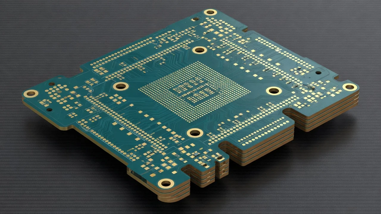
Embedded hardware & firmware
Hybrid circuit boards: mixed-signal, shimmer flex, foldable rigid-flex, mixed-laminate RF, 10-layer HDI. Designed in Altium, brought up on the bench, handed to any CM as Gerbers they can actually build.
Starting $10,000 CAD — a complete test PCB, size and complexity capped below.
01 / ENGINEERED AS ONE
The shape, the signals, the software. We bring them together around the product you want to build, from the first schematic to the factory files.

4–6 layer typical
Bring analog sensing and digital processing onto the same board. Plan the power, signal paths, and layout together, around what your product needs to measure and control.
Sensor platforms / Instrumentation / Connected devices
Hybrid can mean a flexible connection, a mixed-material stackup, or an RF region alongside a digital core. We start with the product’s constraints and agree the construction with the fabricator.
02 / THE BOARD IS ONLY THE BEGINNING
A circuit and its code belong in the same conversation. We connect schematic decisions to behavior you can observe on the bench.
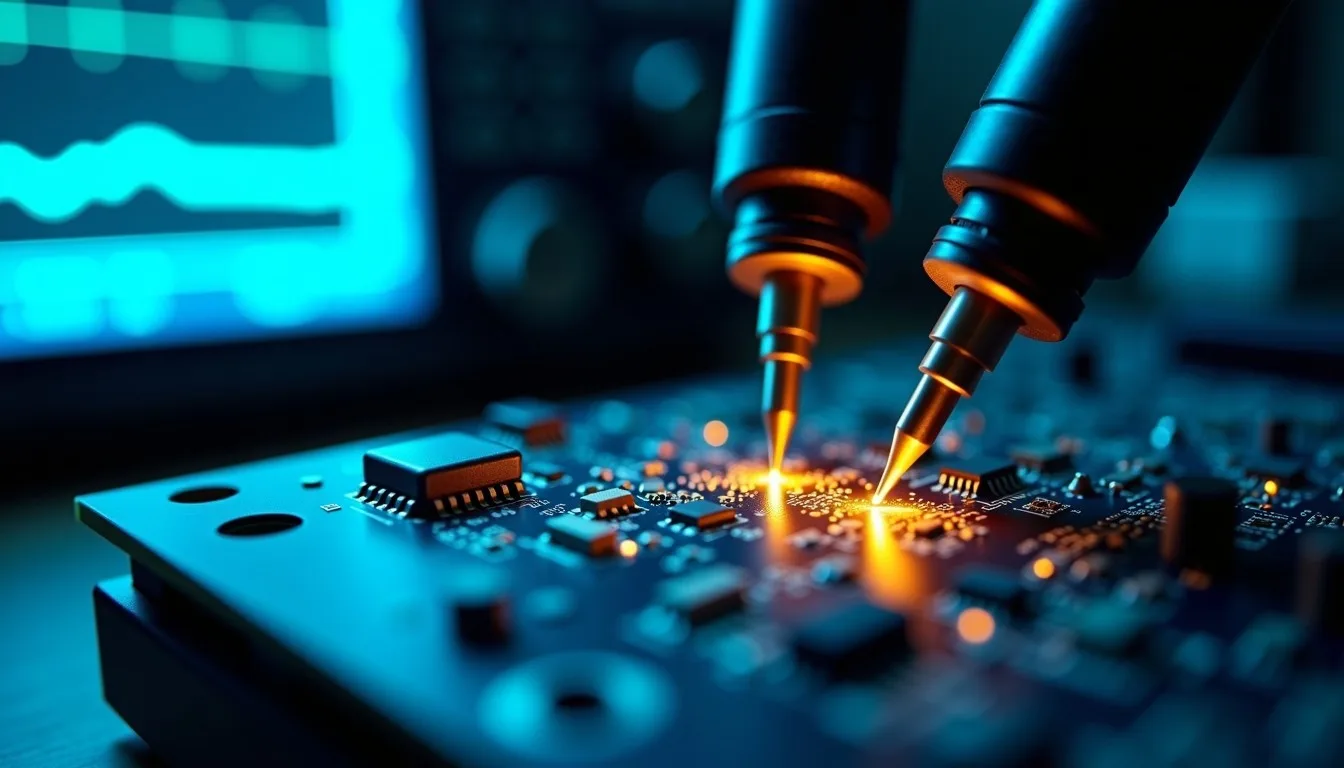 FROM SCHEMATIC TO FIRST SIGNAL
Rail-by-rail bring-up, peripheral checks, and firmware developed against the same schematic. Bench observations feed back into the design.
Bare-metal, FreeRTOS, Zephyr, or embedded Linux. We scope the runtime, interfaces, and power behavior around the device.
Diagnostics, defensive parsing, and update workflows with staged rollout and rollback, where the product requires them.
03 / A CLEAR PLACE TO START
Explore the existing engagement scopes below. Starting prices are in CAD; final scope and schedule are confirmed around your design.
from $10,000 CAD
The entire first custom board: schematic, layout, BOM, fab files, and a short assembled run — brought up on the bench.
Starting design engagements, with the size and complexity limits shown. Fabrication of exotic stackups is quoted with the fab. You own every file.
04 / FROM BENCH TO BUILD
Start with a prototype or bring an existing design. We agree the next milestone and what you need to review before moving forward.
Dev boards, modules, and a focused prototype establish the core behavior.
Prototype & requirementsSchematic, layout, fabrication, and first-board checks connect the design to working hardware.
Custom boards & bench findingsFunctional tests, the certification path, component sourcing, and a pilot build prepare the next step.
Validation & manufacturing reviewEnclosure coordination, tooling, test fixtures, and assembly planning support the production ramp.
Production handoff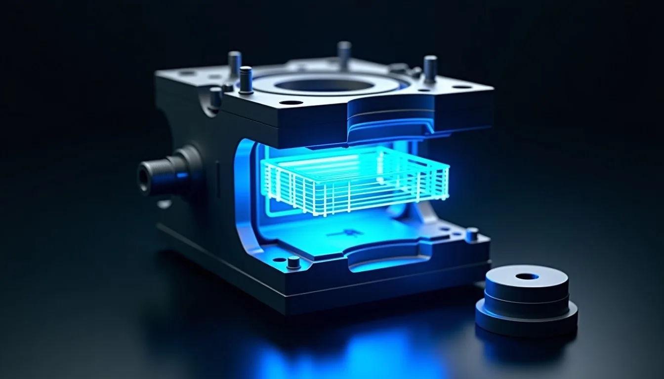
THE BOARD AND THE ENCLOSURE
Board STEP data meets enclosure CAD before tooling is cut. We coordinate manufacturability reviews and tooling quotes with the mold maker, based on the actual part.
05 / BUILT TO BE YOURS
A handoff your team can understand and your manufacturing partner can work with. Editable sources and production outputs, with scope agreed up front.
Manufacturer part numbers, quantities, footprints, lifecycle flags, and approved alternatives where applicable. Your purchasing team gets the context behind the components.
Schematic, PCB, and output-job files for future revisions.
Copper, mask, silkscreen, paste, board outline, and drill data.
Stackup, netlist, and assembly data in the format agreed with the fabricator.
Component position, rotation, and board side for assembly setup.
The design reference for bare-board electrical testing.
Board and component geometry for enclosure coordination.
Yes. A prototype using development boards and off-the-shelf modules can help establish the core behavior before a custom design. Tell us what you need to prove, and we will scope that first step.
We start with the product envelope, signals, power requirements, and manufacturing constraints. A standard rigid board may be enough; flex, rigid-flex, mixed-material, or HDI construction can be explored when the requirements call for it.
Each package lists its starting design price, size or construction limits, indicative timeline, and included outputs. The Test PCB package includes five assembled ENIG prototypes. Fabrication for exotic stackups is quoted with the fabricator. Final scope and schedule are confirmed for your project.
Yes. We can scope hardware design, board bring-up, and firmware together. The package inclusions describe the starting scope; the full firmware requirements, runtime, interfaces, and update needs are agreed separately as part of the proposal.
You own the project files delivered under the engagement. The handoff is scoped to include editable design sources and manufacturing outputs so your team can revise the design and work with a suitable manufacturing partner.
We establish the validation and certification path for the target market and coordinate manufacturing and enclosure requirements. External testing, specialist fabrication, and mold tooling are scoped and quoted for the actual product.
Ready for a hybrid stack?
Tell us the envelope — fold, RF, analog, HDI. We will map it to a class and a starting rate, then propose the engagement.